A Basic Understanding of the Photolithography Process
A casual breakdown of the photolithography process — from photoresist types to clean rooms — by someone genuinely shocked engineering is this hard.
Today I found out what engineering majors actually do
and it really felt like a blessing I didn’t go into engineering.
It seems 20000 times harder than physics. lol lol lol lol lol lol lol lol lol lol lol lol lol lol
Engineering majors, I respect you
lol lol lol this is sick lol lol lol how am I supposed to understand this?? lol lol lol lol
The photolithography process, in Korean, is called “노광기술” (exposure technology). The literal meaning of the word is “light exposure,” meaning to shine light onto something. The reason it is called photolithography is because “lithography (stone-plate printing)” — that is, doing lithography using photons, and the principle is the same as forming an image in a photograph, which is why it’s called photolithography.
The photolithography process refers to processing a designed device pattern on a mask (the mold used to make semiconductors) and implementing it on the wafer (silicon substrate). Also, it does not only encompass the process of forming the image itself, but includes all the processes of transferring a pattern from the mask onto the surface of the silicon wafer. Roughly, that process is
“Cleaning” → Photoresist Coating → Soft Bake → Exposure → Developer → Hard Bake → microscope pattern inspection
so it is said to follow this order. So I’ll try to organize the necessary terms.
Photoresist: it is applied on top of the substrate or thin film to form a photosensitive layer, and is selectively exposed to light through the mask. There are two types: positive photoresist and negative photoresist.
The one that has the property where the part exposed to light dissolves in the developer is called positive photoresist, and the one where the part exposed to light does not dissolve when developed is called negative photoresist.
When using a positive photoresist, compared to using a negative one, it has higher adhesion, better resolution, the film thickness can be made thicker, and since it does not react with oxygen, you can save yourself the trouble of having to react it inside nitrogen gas — these are its advantages. However, when using positive photoresist, because it responds very sensitively to exposure time, you have to stick to the exposure time as sharp as a knife — that’s the drawback.
Now, I’m going to introduce the most rough outline of the photolithography process.
.
- Cleaning
The semiconductor photolithography process has to be carried out in a UV-blocked space (Clean Room), because the PhotoResist (hereafter PR) undergoes polymerization and photodecomposition due to light. It must be performed while checking UV levels, and clean rooms are generally designed as Yellow Rooms.
The cleaning step uses Spin-Coater equipment to apply acetone for cleaning. This is to remove particles and organic matter from the wafer. And then the acetone that has been applied is removed again using methanol.
The principle of the Spin-Coater is as follows.
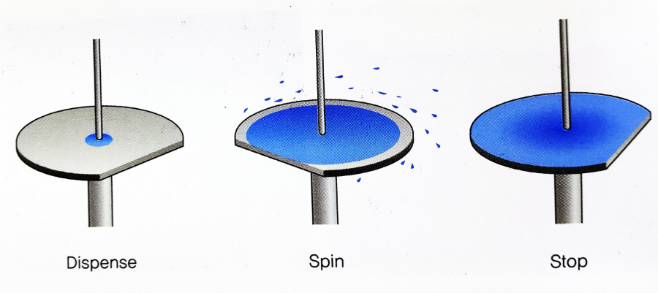
Figure 1. The Spin-Coating process.
- PR Coating
PR is a mixture that has the property of changing its internal structure when exposed to energy such as light, radiation, or heat, so care must be taken.
This is the process of putting PR onto the cleaned wafer. You can’t just coat it any old way — you have to coat it with PR of an appropriate thickness. The PR liquid also typically uses a Spin-Coater device.
Usually, it’s spun for about 30 to 60 seconds, maintaining a rotation speed of around 10005000 rpm. Then the thickness becomes 2.50.5. (The thickness is inversely proportional to the square root of the rotation speed.)
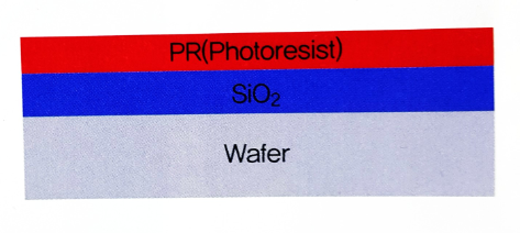
Figure 2. Schematic after PR coating
- Soft-Baking
The soft-baking process is the process of removing the solvent from the PR. This is because if solvent remains, the adhesion with the wafer drops, and also because in the next process, Exposure, the PR’s chemical reaction gets disturbed.
So, through the soft bake process, the solvent is evaporated.
Because the oven that runs the soft baking is well designed, you just need to use the oven, and typically the oven dries at a temperature of 60100 degrees Celsius under nitrogen gas for about 510 minutes.
- Mask Alignment and Exposure
As mentioned before, the mask is the mold for making semiconductors. The mold that has been laid out has to be arranged ‘well’. Arranging it well means operating the microscope and using the micrometer to Align it. And after going through proper exposure, the pattern of the mask gets transferred onto the PR.
When exposing, there are roughly 3 kinds of Align Contact Mode methods. There’s ‘Soft Contact’, ‘Vacuum Contact’, ‘Hard Contact’, and ‘Proximity’. Soft contact is the method of raising the stage (substrate) to contact the mask and the wafer. Vacuum contact is the method of evacuating the space between the wafer and the mask to raise the adhesion and bring them into contact. Hard contact is the method of using nitrogen gas to raise the adhesion, and lastly, Proximity is the method of deliberately giving a gap between the mask and the wafer during exposure. Proximity is the method used when it’s carried out for special purposes such as preventing contamination.
- Development
After exposure, the pattern that existed on the mask gets transferred, divided into the polymerized parts of the PR layer and the parts that are not.
The development step is precisely the step of removing these non-polymerized parts.
As for the methods, there are Immersion and spray methods. For Immersion, you just dip the wafer into the developer, then dip it again into the rinse solution container, and then dry it. The Spray method is spraying it by spin coating, the same as when coating the PR.
- Hard-Baking (Lift-off)
This is the step of evaporating the solvent once more to improve adhesion. The hardness is raised, improving durability.
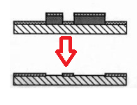
Figure 3. Lift-off
In <figure 3.>, the lower process is what it looks like after the hard baking process.
This process also just uses the hard bake device, and the hard bake device operation is carried out for about 5 minutes at roughly 110 degrees.
- Measurement
Since the formation of the pattern has all been completed, this is the process of measuring and evaluating the 3D shape by mobilizing 3D Laser microscope equipment.
First, the wafer is washed using BOE (Buffered Oxide Etch) solution. And after rinsing using ultrapure water, it is dried using nitrogen or the like. And then, after measuring using a 3D Laser, an analysis program is used to analyze and evaluate things like the line width of the pattern.
References
[1] Richard C. Jaeger, Lee Sang-ryeol, Myung Jae-min, Yoon Il-gu, Introduction to Semiconductor Processing, Kyobo Book Centre (2002)
[2] Lee Byung-ryeol, Yoon Seok-il, Semiconductor Process Practice, Hongreung Science Publishing (2015)
[3] Hwang Ho-jung, Semiconductor Process Technology, Saengneung Publishing (2005)
[4]. Samsung Semiconductor Story, http://www.samsungsemiconstory.com, 16. 3.22.
Originally written in Korean on my Naver blog (2016-03). Translated to English for gdpark.blog.